


Business ExpandingGENESINK, Developer of Conductive Ink, Establishes an Office in Aichi Prefecture
Mar 19, 2026
GENESINK![]() is a French company engaged in the development and manufacturing of high-performance conductive and semi-conductive inks.
is a French company engaged in the development and manufacturing of high-performance conductive and semi-conductive inks.
- Establishment
- 2025/10
- Destination
- Aichi , Nagoya city
- Semiconductors, Robotics, and Machinery
-
France

Founded in 2010, GENESINK specializes in the research, formulation, and co-industrialization of nanomaterial-based solutions to address miniaturization, electromagnetic interference, and durability challenges in cutting-edge electronics.
The company enables the printing of thin, lightweight, secure, and energy-efficient electronic circuits and functional layers designed for easy integration into complex systems while addressing multiphysics constraints.
Its portfolio includes ultra-conductive silver-based inks powering compact architectures, semiconductor inks enabling functionalization and charge transfer, and conductive transparent inks.
Compatible with most printing methods and advanced substrates, particularly flexible and heat-sensitive ones, GENESINK’s products unlock key innovations in medtech, perovskite photovoltaics, smart glass, and other strategic industries. The company’s advanced materials design capabilities also demonstrate strong potential for applications in the advanced semiconductor field and have earned international recognition.
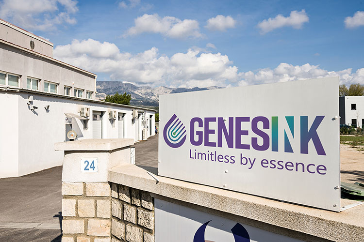
Exterior Premises and panel
Through additive printing approaches, these inks significantly reduce material loss and energy consumption compared with conventional etching and vacuum deposition processes, making them a highly regarded technology contributing to more sustainable electronic device manufacturing.
Beyond its standard portfolio, the company provides formulation customization, process engineering guidance, and licensing to facilitate industrial integration and scale-up.
To strengthen its business development and customer support in the Japanese market, GENESINK established a representative office in Nagoya, Aichi Prefecture, in October 2025.
In connection with the establishment of its Japan office, JETRO’s Invest Japan Business Support Center (IBSC) provided a wide range of support, including consultations on registration, taxation, and labor matters, PR assistance, business matching, access to IBSC facilities, and the introduction of office properties.
Going forward, the company plans to deepen collaboration with major domestic semiconductor manufacturers and accelerate the implementation of its high-performance materials in the Japanese market.
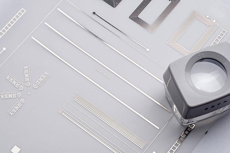
Screen printing on PET and a measuring loupe
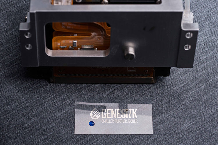
GNK circuit and printhead
JETRO supports your business in Japan
JETRO IBSCs are located in Japan's major business hubs and provide one-stop support and service to foreign firms seeking to set up or expand business in Japan. The centers, which provide free temporary office space, consultation with expert advisors and access to a wealth of business information, tailor support according to the specific needs and phase of development of each firm.

Contact Us
Investing in and collaborating with Japan
We will do our very best to support your business expansion into and within Japan as well as business collaboration with Japanese companies. Please feel free to contact us via the form below for any inquiries.
Inquiry FormJETRO Worldwide
Our network covers over 50 countries worldwide. You can contact us at one of our local offices near you for consultation.
Worldwide Offices